Positive Edge Triggered D Flip Flop Timing Diagram. Thus the output has two stable states based on the inputs which have been discussed below. A timing diagram illustrating the action of a positive edge triggered device is shown in fig.
Jk flip flop circuit in order to have an insight over the working of jk flip flop it has to be realized in terms of basic gates similar to that in figure 2 which expresses. Thus the output has two stable states based on the inputs which have been discussed below. Truth table of d flip flop.
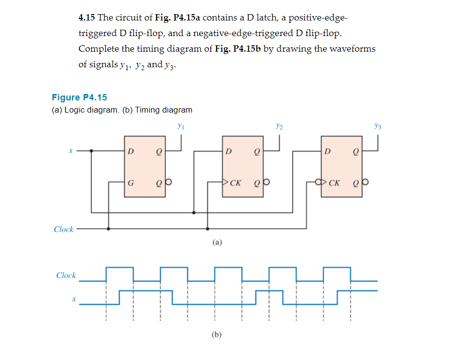
Again this gets divided into positive edge triggered d flip flop and negative edge triggered d flip flop.
Again this gets divided into positive edge triggered d flip flop and negative edge triggered d flip flop. Positive edge triggered d flip flop on the positive edge while the clock is going from 0 to 1 the input d is read and almost immediately propagated to the output q. Just before pulse c the d input goes low so at the positive going edge of pulse c q goes low. D flip flop.
