Parallel Binary Adder Block Diagram. Cout a nbits nbits s b nbits cin fig. Full adder and parallel binary adder 159 table 181 pin assignments for a full from soc 490 590 at south dakota state university.
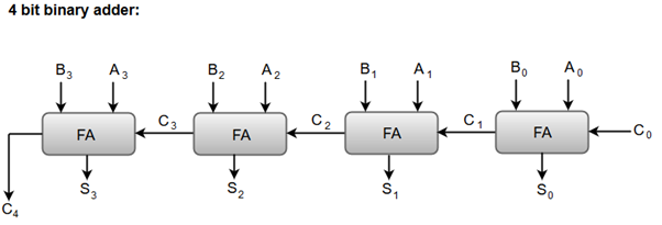
In the block diagram a0 and b0 represent the lsb of the four bit words a and b. In the 4 bit adder first block is a half adder that has two inputs as a0b0 and produces their sum s0 and a carry bit c1. Parallel adders are digital circuits that compute the addition of variable binary strings of equivalent or different size in parallel.
The carry output of the previous full adder is connected to carry input of the next full adder.
For 4 bit binary numbers a and b of the form a. This parallel adder produces their sum as c4s3s2s1s0 where c4 is the final carry. Parallel adder circuit diagram jul 07 2020 the below block diagram shows n number of full adders cascaded with one another to design a n bit parallel adder. As you can see in the diagram a n a 2 a 1 a 0 and b n b 2 b 1 b 0 are the n bit binary digits which are to be added.
