Jk Flip Flop Timing Diagram Calculator. The s and r inputs of the rs bistable have been replaced by the two inputs called the j and k input respectively. In addition to the basic input output pins shown in figure 1 j k flip flops can also have special inputs like clear clr and preset pr figure 4.
The timing pulse must be very short because a change in q before the clock pulse goes off can drive the circuit into an oscillation called racing modern ics are so fast that this simple version of the j k flip flop is not practical we put one together in the. When j 0 k 1 the output is set to low. When j 1 k 0 the output is set to high.
Mungkin kalian keluar soal ini jadi udah latihan dulu mohon maaf apabila ada salah kata atau perbuatan ya.
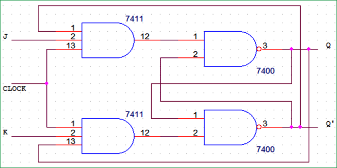
Jk flip flop construction logic circuit diagram logic symbol truth table characteristic equation excitation table are discussed. Jk flip flop circuit diagram and explanation. The s and r inputs of the rs bistable have been replaced by the two inputs called the j and k input respectively. Also we have used led at output the source has been limited to 5v to control the supply voltage and dc output voltage.
