Cmos Inverter Vtc. The body effect is not present in either device since the body of each device is directly connected to the device s source. The effect of nbti mainly impacts the p channel mosfet right hand side transistor.
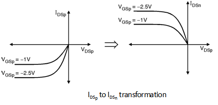
Brief introduction to cmos logic gates intro to chapter 6 mostransistor chapter3 eecs141ee141 3 mos transistor chapter 3 today s lecture mos transistor chapter 3 reading 3 3 1 3 3 2 5 1 5 3 cmos inverter eecs141ee141 4 vtc the cmos inverter vi v t vdd eecs141ee141 5 n ou vout idn pmos load lines vin vdd vgsp idn idp vout. The top fet mp is a pmos type device while the bottom fet mn is an nmos type. The above figure shows the voltage transfer characteristics of the cmos inverter.
Dc analysis of cmos inverter egat lo vtupn i n vi vout output voltage single power supply vdd ground reference find vout f vin voltage transfer characteristic vtc plot of vout as a function of vin vary vin from 0 to vdd find vout at each value of vin.
The body effect is not present in either device since the body of each device is directly connected to the device s source. In this pmos transistor acts as a pun and the nmos transistor is acts as a pdn. Inverter vtc reading 5 1 5 3 ee141 4 eecs141 lecture 10 4 cmos inverter vtc ee141 5 eecs141 lecture 10 5 the cmos inverter vin vout vdd wp βwn wn ee141 6 eecs141 lecture 10 6 pmos load lines for dc vtc i dn i dp graphically looking for intersections of nmos and pmos iv characteristics to put iv curves on the. Brief introduction to cmos logic gates intro to chapter 6 mostransistor chapter3 eecs141ee141 3 mos transistor chapter 3 today s lecture mos transistor chapter 3 reading 3 3 1 3 3 2 5 1 5 3 cmos inverter eecs141ee141 4 vtc the cmos inverter vi v t vdd eecs141ee141 5 n ou vout idn pmos load lines vin vdd vgsp idn idp vout.
